With product standards and safety requirements so crucial, the highest quality standard of sensors and monitoring is imperative. ION Science, leaders in PID (photoionization detection) technology are experienced in delivering volatile organic compound (VOC) detector solutions.
Semiconductors have changed the way we live and continue to play a key role in our future. As the number of production facilities increase, so the potential for harmful emissions also rises. Sensor technology supports the semiconductor industry by enabling consistency and uniformity, while at the same time protecting those working directly on the fabrication process, and off-site emissions that can potentially impact local communities.
Demand for semiconductors is at an all-time high with a wide spectrum of usage including smartphones on a small scale, electric cars on the medium scale and within smart factories on an industrial scale. Whatever their end application, they require extremely precise fabrication.
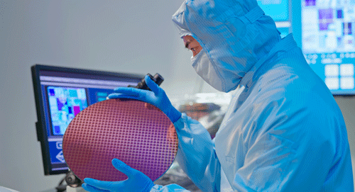
Different types of VOCs (volatile organic compounds) and gases are used in the development of integrated circuits on silicon wafers. Determining and ensuring the exact amount of VOC exposure is crucial, both for consistency and for personal health. Unaccounted-for VOCs have the potential to interfere with the creation of a wafer and ruin a circuit, potentially even a whole batch.
Ensuring consistent performance on a product line cannot be underestimated. By incorrectly monitoring VOCs and gases, businesses run the risk of wasting vital resources and damaging the health of those employed to manufacture them.
Workers are at risk of being exposed to VOCs used and highly toxic VOCs generated as by-products during the fabrication process. Devices are produced in clean rooms that are strictly controlled to avoid the generation and deposition of particles on wafers. Fabrication facilities are generally equipped with local associated ventilation systems to help manage VOCs. However, in some facilities, the air exposed to the photolithography process is only recirculated with 20 – 30 % outdoor air therefore allowing low concentrations of VOCs to potentially persist.Workers are at risk of being exposed to VOCs used and highly toxic VOCs generated as by-products during the fabrication process.
Devices are produced in clean rooms that are strictly controlled to avoid the generation and deposition of particles on wafers. Fabrication facilities are generally equipped with local associated ventilation systems to help manage VOCs. However, in some facilities, the air exposed to the photolithography process is only recirculated with 20 – 30 % outdoor air therefore allowing low concentrations of VOCs to potentially persist.
In addition to personal safety and product consistency, other major factors behind the importance of accurate sensor monitoring are the environmental and financial elements. A whole batch of semiconductors ruined due to over-exposure to VOCs can mean a large wastage of products, which can cause both environmental and sustainability issues. With such a shortage of semiconductors globally, preventing product loss through VOC detection is an easy way to maintain supply chains.
When accurately monitored by high precision sensors, VOCs and gases used in the semiconductor industry do not need to be detrimental to human health. However, without consistent and accurate measurement, such as that provided by ION Science sensors, worker risk is significantly increased due to potential exposures to a variety of chemicals above safe concentrations for extended periods.
The types of VOCs that workers could potentially be exposed to include ethylene glycol, trichloroethylene, and xylene. There is also a potential risk of benzene and formaldehyde exposure because of certain processes. Even in lower concentrations these can pose significant health risks. Monitoring for VOCs and protecting the health of workers takes a high priority and is why clear guidelines for exposure are laid out and need to be accurately analysed by sensors.


